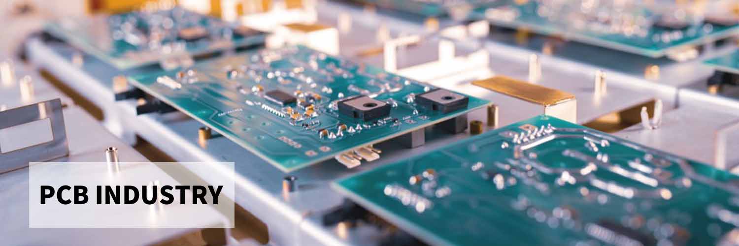
PCB Industry
Industry Overview
The PCB (Printed Circuit Board) industry is the foundational backbone of modern electronics, enabling connectivity and functionality across 3C electronics, automotive, communication, medical, and industrial applications. As devices evolve toward miniaturization, high-frequency signal transmission, and multilayer integration, PCB manufacturing requires increasingly precise, efficient, and clean processing technologies.
Laser technology, with its non-contact, precise, and adaptive advantages, is rapidly becoming the go-to solution for drilling, cutting, marking, and surface treatment in advanced PCB production.
Industry Challenges
Micron-level precision in drilling micro-vias, especially for HDI and flexible PCBs
Delicate substrates (e.g., polyimide, LCP, CCL, ceramics) sensitive to heat and deformation
Complex board structures: Rigid-flex, multilayer, or ultra-thin materials require flexible tooling
Environmental regulations demand cleaner, chemical-free processes
Need for traceability and automated integration with smart production lines
Laser Solutions for the PCB Industry
Laser Drilling Solutions
Applications: Blind/buried vias, through-holes in FPCs, micro-vias in HDI boards
Advantages: High precision (<20μm), no tool wear, suitable for high-speed inline production
Recommended Systems: UV Laser Drilling Machine, CO₂ Laser Via Drilling System
Laser Cutting & Profiling
Use Cases: PCB outline cutting, depaneling, flex board trimming, rigid-flex separation
Benefits: Burr-free, minimal charring, supports tight layouts and complex contours
Recommended Products: UV Laser Cutter, Femtosecond Laser Cutting Platform
Laser Marking for Traceability
Applications: QR code/serial number marking on PCBs, FPCs, ceramic boards
Advantages: High contrast, minimal material ablation, non-damaging to circuits
Recommended Products: UV Laser Marking Machine, Green Laser PCB Marker
Laser Surface Cleaning / Etching
Target Scenes: Surface oxide removal, copper residue cleaning, solder mask pre-treatment
Process Benefits: No chemical waste, no damage to substrate, cleanroom compatible
Recommended Products: UV Laser Cleaning Machine, Pico Laser Surface Processor
Application Examples
| PROJECT | LASER PROCESS |
|---|---|
| Blind via drilling in HDI board | UV laser drilling |
| QR code engraving on rigid-flex PCB | UV laser marking |
| Depaneling of flexible circuits | UV laser cutting |
| Cleaning copper oxide from pad areas | Laser surface cleaning |
| Scribing of ultra-thin ceramic substrates | Femtosecond laser cutting |
Industry Trends
High-Density & Miniaturized PCBs: Laser enables precise micromachining for 5G/IoT/AI chips
Flexible & Wearable Electronics: PCB design shifts toward thin, flexible substrates with tight tolerance
Green, Clean Manufacturing: Laser replaces wet etching and mechanical drilling
Smart Factories & Digital Traceability: PCB production is becoming more traceable and automated
Cooperation Models
Provide full laser systems or customized modular units for PCB production lines
Deliver technical support, installation & commissioning, operator training
Support OEM/ODM partnerships to meet your application, branding, and integration needs
Let Us Empower Your PCB Manufacturing
From HDI micro-vias to flexible PCB profiling, our laser systems ensure ultra-precise, clean, and efficient production to help you scale for next-generation electronics.
Contact our technical team to customize a solution based on your board structure, daily output, and production workflow.

