Introduction to Deep UV Laser Technology
Deep ultraviolet (DUV) laser technology represents one of the most significant advancements in precision manufacturing, particularly within the semiconductor industry. Operating at wavelengths between 200-280nm, with 266nm being a particularly important wavelength, deep UV lasers enable material processing capabilities that were previously impossible with conventional laser systems. As semiconductor devices continue to shrink toward nanometer-scale features, the demand for precise, non-thermal processing methods has driven rapid adoption of deep UV laser technology across the industry.
The unique characteristics of UV laser source systems operating in the deep ultraviolet range make them indispensable for applications requiring minimal thermal damage, high precision, and compatibility with sensitive semiconductor materials. Unlike longer wavelength lasers that rely on thermal ablation, deep UV lasers achieve material removal through photochemical processes, preserving the integrity of surrounding structures.
Fundamental Principles of Deep UV Laser Processing
Photochemical vs. Thermal Ablation
Traditional laser processing relies on thermal ablation, where absorbed laser energy heats the material until it vaporizes. This thermal process creates heat-affected zones that can damage sensitive semiconductor structures. Deep UV lasers operate differently—their high-energy photons directly break molecular bonds without significant heating, a process known as photochemical ablation or “cold ablation.”
This fundamental difference enables processing of temperature-sensitive materials and structures common in semiconductor manufacturing. For instance, polymers used in photoresist applications can be precisely patterned without thermal deformation, while semiconductor wafers can be processed without introducing thermal stress that might affect device performance.
Wavelength Selection and Material Interaction
The 266nm wavelength, achieved through frequency quadrupling of Nd:YAG or Nd:YVO4 lasers, offers optimal characteristics for semiconductor processing. At this wavelength, many materials exhibit strong absorption, enabling efficient processing with minimal penetration depth. This shallow absorption ensures precise material removal with excellent depth control.
Material-specific absorption characteristics determine processing efficiency and quality. Silicon, silicon dioxide, various polymers, and metals each respond differently to deep UV laser energy. Understanding these interactions is essential for optimizing processing parameters and achieving desired results in semiconductor manufacturing applications.
Key Applications in Semiconductor Manufacturing
Photomask Repair and Defect Correction
Photomask repair represents one of the most demanding applications for laser source technology in semiconductor manufacturing. As feature sizes shrink below 10nm, even sub-nanometer defects can render a photomask unusable. Deep UV laser systems provide the precision necessary to remove or repair these defects without damaging surrounding patterns.
Advanced photomask repair systems combine deep UV laser processing with precision positioning and real-time inspection capabilities. These systems can identify defects, plan repair strategies, and execute repairs with nanometer-scale accuracy, enabling the production of defect-free photomasks for advanced lithography processes.
Wafer Dicing and Scribing
Traditional mechanical dicing methods introduce stress and contamination that become increasingly problematic as die sizes shrink. picosecond laser and deep UV laser dicing offers a non-contact alternative that eliminates mechanical stress while providing clean, precise cuts. The cold ablation process minimizes debris and thermal damage, improving die yield and reliability.
Laser scribing processes create controlled fracture lines that enable clean die separation without the material loss associated with traditional saw dicing. This technique is particularly valuable for thin wafers and sensitive materials where mechanical methods would cause unacceptable damage.
Thin Film Patterning
Thin film patterning for semiconductor devices requires precise removal of material layers without damaging underlying structures. Deep UV lasers excel at this application, offering selective material removal with minimal thermal impact. The technology enables patterning of conductive layers, dielectric materials, and barrier films with sub-micron precision.
Applications include patterning of transparent conductive oxides for display manufacturing, removing anti-reflective coatings in photovoltaic cell production, and creating fine-line circuit patterns for advanced packaging applications. Each application benefits from the precise, non-thermal processing characteristics of deep UV laser technology.
Through-Silicon Via (TSV) Formation
Three-dimensional integrated circuits require vertical interconnects through silicon wafers, known as through-silicon vias. Creating these vias with high aspect ratios and minimal damage requires precise laser drilling capabilities. Deep UV lasers enable the creation of small-diameter vias with clean sidewalls and minimal thermal damage to surrounding material.
The non-thermal processing nature of deep UV lasers is particularly valuable for TSV formation, as thermal damage could affect the electrical characteristics of nearby devices. Combined with appropriate beam delivery and motion control systems, deep UV lasers can create thousands of vias per second with consistent quality.
Technical Considerations for Implementation
Laser Source Selection
Selecting the appropriate laser source requires consideration of wavelength, pulse duration, average power, and beam quality. For deep UV applications, the choice between frequency-converted solid-state lasers and direct UV sources affects system complexity, maintenance requirements, and processing capabilities.
Frequency-quadrupled lasers generating 266nm output offer excellent beam quality and precise control over pulse parameters. However, the frequency conversion process introduces efficiency losses and requires careful thermal management. Direct UV sources, while potentially simpler, may offer different characteristics that affect processing outcomes.
Beam Delivery and Optics
Deep UV wavelengths require specialized optical materials and coatings. Standard optical glasses may absorb UV radiation, leading to heating and damage. UV-grade fused silica, calcium fluoride, and other specialized materials enable efficient beam delivery at deep UV wavelengths.
Beam delivery systems must maintain precise focus and beam quality over the working area. Galvanometer scanners, precision linear stages, and advanced focusing optics combine to enable rapid, accurate positioning of the laser spot. Integration with vision systems enables real-time alignment and quality monitoring.
Environmental Control
Deep UV processing typically requires controlled atmospheric conditions. Ambient oxygen can absorb UV radiation, reducing processing efficiency. Additionally, some materials produce hazardous byproducts when processed with UV lasers. Enclosed processing environments with appropriate gas flow and filtration protect both the process and operators.
Cleanroom compatibility is essential for semiconductor manufacturing applications. Laser systems must be designed to minimize particle generation and integrate seamlessly with cleanroom protocols. This includes sealed beam paths, filtered exhaust systems, and compatibility with cleanroom-compatible materials.
Integration with Manufacturing Systems
Automation and Process Control
Modern semiconductor manufacturing demands highly automated processes with minimal human intervention. Deep UV laser systems integrate with factory automation systems through standardized interfaces and protocols. Process recipes stored in manufacturing execution systems enable rapid changeover between different products and processes.
In-line metrology systems verify process quality in real-time, enabling immediate feedback and adjustment. This closed-loop control ensures consistent quality across production lots while maximizing throughput and yield. Statistical process control methods track key parameters and identify trends that might indicate developing issues.
Quality Assurance and Yield Optimization
Process qualification for deep UV laser operations typically involves extensive characterization of process windows and capability indices. Understanding the relationships between laser parameters, material properties, and process outcomes enables optimization for maximum yield and throughput.
Advanced process monitoring systems track laser energy, pulse characteristics, and beam position in real-time. Any deviation from specified parameters triggers automatic process adjustment or lot holds, preventing the production of defective products. This proactive approach to quality assurance is essential for the high-value products characteristic of semiconductor manufacturing.
Future Developments and Industry Trends
Continued Wavelength Reduction
As semiconductor features continue to shrink, shorter wavelengths become increasingly attractive. Research into extreme UV (EUV) sources at 13.5nm has already enabled production of devices with sub-10nm features. The integration of these sources into manufacturing systems presents significant technical challenges but offers substantial benefits for advanced device production.
Increased Process Speed and Throughput
Manufacturing economics drive continuous improvement in process throughput. Higher power laser sources, faster beam positioning systems, and improved process efficiency all contribute to increased throughput. Multi-beam processing approaches offer multiplicative improvements in process speed by simultaneously processing multiple sites.
Advanced Process Monitoring and Control
Artificial intelligence and machine learning are being applied to laser process optimization and control. These technologies enable prediction of optimal processing parameters, detection of subtle quality variations, and automatic compensation for process drift. As these technologies mature, they will enable even more precise and reliable deep UV laser processing.
Conclusion
Deep UV laser technology has become an essential tool in semiconductor manufacturing, enabling precise, non-thermal processing of sensitive materials and structures. From photomask repair to wafer dicing and thin film patterning, deep UV lasers provide capabilities that traditional methods cannot match. As the semiconductor industry continues to advance toward smaller features and more complex devices, the importance of deep UV laser technology will only increase.
Successful implementation requires careful consideration of laser source characteristics, beam delivery systems, environmental controls, and integration with manufacturing automation. The investment in appropriate technology and expertise pays dividends through improved yield, enhanced device performance, and access to manufacturing capabilities that enable next-generation semiconductor products.
For manufacturers seeking to implement deep UV laser processing, partnerships with experienced laser technology providers offer valuable support in system design, process development, and ongoing optimization. The combination of advanced laser hardware and application expertise enables rapid deployment of production-ready solutions that meet the demanding requirements of semiconductor manufacturing.

2026 Mid-Autumn Festival and National Day Holiday Notice
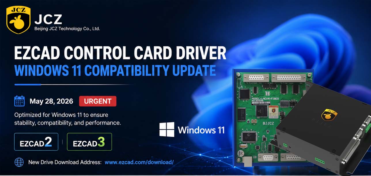
OFFICIAL DRIVER UPDATE NOTICE

Top Factors That Affect Marking Quality in Handheld Fiber Laser Systems

Meet JCZ at Laser World of Photonics India 2026 in Bengaluru
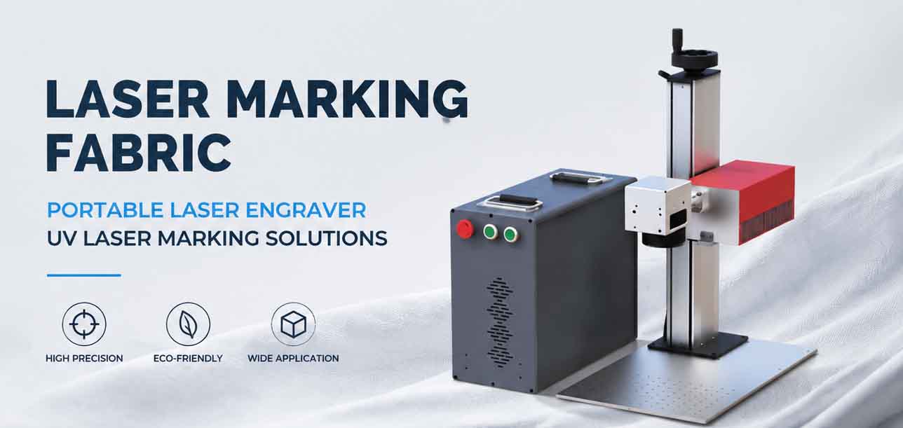
Laser Marking Fabric with Portable Laser Engraver: Advanced UV Laser Marking Solutions for Modern Manufacturing
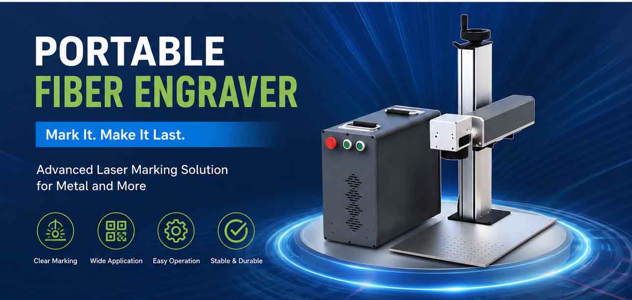
Laser Machine for Marking: The Ultimate Guide to Portable Fiber Engravers & MOPA Color Laser Marking